
"SI WAFER, TYPE P, 4"""
Ø4" Silicon Wafer, Type P / <100>
- Art no: 16010
- Weight: 0
- Qty: st
Description
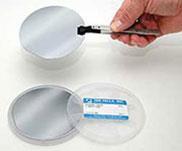
These 1", 2", 3", 4" and 6" diameter silicon wafers can be used either as a substrate for thin film research or to make small silicon substrates by dicing the wafer into smaller pieces using a scriber and the Wafer Cleaving / Glass Breaking Pliers. The wafer is shipped in a wafer carrier.
Properties:
- Orientation: <100> for 1", 2", 4"and 6" wafer <111> for 3"
- Resistance: 1-30 Ohms
- Type P: (Boron) (1 primary flat)
- No SiO2 top coating
- Wafer thickness:
Ø1" = 10 - 12 mill (254 - 304 µm)
Ø2" = 9 - 13 mill (230 - 330 µm)
Ø3" = 13.6 - 18.5 mill (345 - 470 µm)
Ø4" = 18.7 - 22.6 mill (475 - 575 µm)
Ø6" = 23.6 - 25.2 mill (600 - 690 µm)
- Roughness: 2nm
- TTV: = <20µm
- Wafer is polished on one side
See


Tillagd i varukorgen