
BSE Atomic Reference Specimen
An electron microscope, when equipped with a backscattered electron detector, has the capability to produce images in which the contrast is controlled by differences in atomic number (Z) across the specimen. Four reference specimens are now available that are suitable for testing the atomic number contrast performance of a backscattered electron detection system.
Each of the reference specimens consists of two high purity elements that have an atomic number difference of 1. They are in the form of two wires embedded side by side in a contrasting matrix.
The specimens are available as a single mount either 3mm or 5mm diameter brass or aluminium tubes or alternatively can be incorporated into a block of standards.
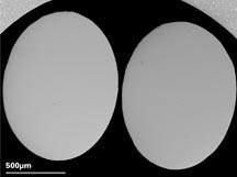
Electron micrograph of the nickel/copper backscattered electron reference specimen. BSE image at low magnification.
The contrast difference between the two wires is visible due to the atomic number difference between the nickel/copper.
For ordering:
Art# 652 BSE Atomic Reference, Nickel (Z-28) - Copper (Z-29)
Art#653 BSE Atomic Reference, Palladium (Z-46) - Silver (Z-47)
Art# 654 BSE Atomic Reference, Platinum (Z-78) - Gold (Z-79)
Duplex Reference Specimen
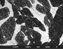
An alternative and very sensitive test is by means of an alloy with two major copper/zinc phases separated by an atomic number difference of 0.1. The light phase illustrated in the micrograph has a mean atomic number of 29.47 and the dark phase a mean atomic number of 29.37.
For ordering:
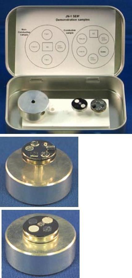
JN-1 SEM Demonstration Specimens
The JN-1 Scanning Electron Microscope Demonstration Standard Specimen demonstration samples on two standard 12.7mm (1/2") pin stubs and a 25mm mounting adapter.
They allow for demonstrating any SEM at lower magnifications with known specimens. The variety of demonstration samples can also be used for training purposes.
They are ideal for use on table top SEMs such as the JEOL NeoScope, Hitachi TM-1000/3000/3030, Phenom and Agilent / Keysight 8500 FE-SEM.
The JN-1 SEM Demonstration Standard is not intended for magnification calibration.
The pin stubs are directly compatible with SEMS made by FEI/Philips, Zeiss/LEO, Cambridge Instruments/Leica, Tescan, CamScan, Amray, Agilent and Aspex.
The 25mm (1") cylinder stub adapter holds the pin of the pin stub with a spring loaded set screw and does not require tools to secure the pin stub. The cylinder adapter is compatible with virtually all JEOL and Hitachi SEMs. On the bottom of the cylinder there is a 4mm internal thread compatible with Hitachi SEMs. It is recommended to handle the pin stubs with pin stub grippers which will fit the groove on the pin stubs. Store the SEM demonstration standard in a dust-free and dry environment.
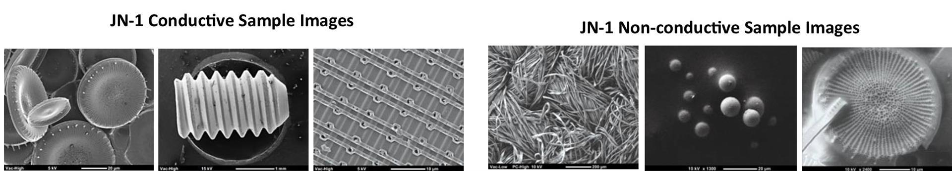
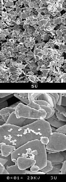
One pin stub contains six conductive samples including, an integrated circuit chip, metal spheres, small set screw, ductile steel fracture, diatoms and a TEM grid. The entire stub is coated with ~20nm of Au:Pd to ensure conductivity on all samples.
The second stub contains five non-conductive samples including an integrated circuit chip, paper, glass spheres, fabric and diatoms.
This stub is not coated for conductivity and is useful to demonstrated low-vacuum SEM imaging, charging and back-scattered electron imaging.
For ordering:
PELCO® Astigmatism Corrector
Clear, sharp, high contrast images easy to stigmate and use for checking resolution.
Sharp-edged gold particles supported on a 3mm diameter 1000 mesh copper TEM grid attached to any specimen mount of the group listed below.
This specimen is used to:
1. determine the presence of astigmatism and allow correction2. determine instrument resolution.
See drawings to identify specimen mount and the correct ordering number. The specimen may also be prepared on a custom mount of your choice.
For ordering:
Art#640 PELCO® Astigmatism Corrector
See the #16179 PELCO® SEM Sample Stub Vacuum Desiccator
See information on mounts A-Q